- 您现在的位置:买卖IC网 > Sheet目录2006 > LTC2435CGN#TRPBF (Linear Technology)IC ADC DIFF I/REF 20BIT 16-SSOP
LTC2435/LTC2435-1
2
24351fc
For more information www.linear.com/LTC2435
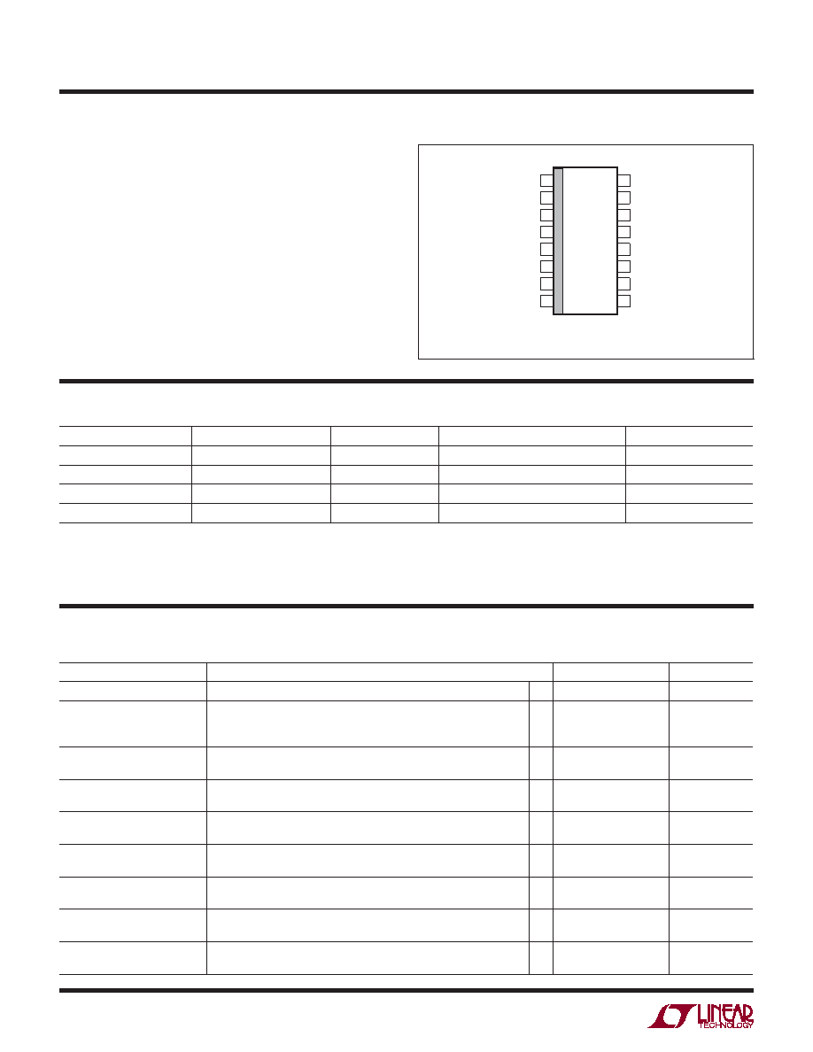
pin conFiguraTion
absoluTe MaxiMuM raTings
Supply Voltage (VCC) to GND.......................–0.3V to 7V
Analog Input Pins Voltage to GND –0.3V to (VCC + 0.3V)
Reference Input Pins Voltage
to GND ..........................................–0.3V to (VCC + 0.3V)
Digital Input Voltage to GND .........–0.3V to (VCC + 0.3V)
Digital Output Voltage to GND.......–0.3V to (VCC + 0.3V)
Operating Temperature Range
LTC2435C/LTC2435-1C ........................... 0°C to 70°C
LTC2435I/LTC2435-1I ......................... –40°C to 85°C
Storage Temperature Range................... –65°C to 150°C
Lead Temperature (Soldering, 10 sec) .................. 300°C
(Notes 1, 2)
TOP VIEW
GN PACKAGE
16-LEAD PLASTIC SSOP
1
2
3
4
5
6
7
8
16
15
14
13
12
11
10
9
GND
VCC
REF+
REF–
IN+
IN–
GND
FO
SCK
SDO
CS
GND
TJMAX = 125°C, θJA = 95°C/W
orDer inForMaTion
LEAD FREE FINISH
TAPE AND REEL
PART MARKING
PACKAGE DESCRIPTION
TEMPERATURE RANGE
LTC2435CGN#PBF
LTC2435CGN#TRPBF
2435
16-Lead Plastic SSOP
0°C to 70°C
LTC2435IGN#PBF
LTC2435CGN#TRPBF
2435I
16-Lead Plastic SSOP
–40°C to 85°C
LTC2435-1CGN#PBF
LTC2435-1CGN#TRPBF
24351
16-Lead Plastic SSOP
0°C to 70°C
LTC2435-1IGN#PBF
LTC2435-1IGN#TRPBF
24351I
16-Lead Plastic SSOP
–40°C to 85°C
Consult LTC Marketing for parts specified with wider operating temperature ranges.
Consult LTC Marketing for information on nonstandard lead based finish parts.
For more information on lead free part marking, go to: http://www.linear.com/leadfree/
For more information on tape and reel specifications, go to: http://www.linear.com/tapeandreel/
elecTrical characTerisTics The
l
denotes specifications which apply over the full operating
temperature range, otherwise specifications are at TA = 25°C. (Notes 3, 4)
PARAMETER
CONDITIONS
MIN
TYP
MAX
UNITS
Resolution (No Missing Codes) 0.1V ≤ VREF ≤ VCC, –0.5 VREF ≤ VIN ≤ 0.5 VREF , (Note 5)
●
20
Bits
Integral Nonlinearity
5V ≤ VCC ≤ 5.5V, REF+ = 2.5V, REF– = GND, VINCM = 1.25V, (Note 6)
5V ≤ VCC ≤ 5.5V, REF+ = 5V, REF– = GND, VINCM = 2.5V, (Note 6)
2.7V ≤ VCC ≤ 5.5V, REF+ = 2.5V, REF– = GND, VINCM = 1.25V, (Note 6)
●
2
3
10
20
ppm of VREF
Offset Error
2.5V ≤ REF+ ≤ VCC, REF– = GND,
GND ≤ IN+ = IN– ≤ VCC, (Note 14)
●
2
5
mV
Offset Error Drift
2.5V ≤ REF+ ≤ VCC, REF– = GND,
GND ≤ IN+ = IN– ≤ VCC
100
nV/°C
Positive Gain Error
2.5V ≤ REF+ ≤ VCC, REF– = GND,
IN+ = 0.75REF+, IN– = 0.25 REF+
●
10
25
ppm of VREF
Positive Gain Error Drift
2.5V ≤ REF+ ≤ VCC, REF– = GND,
IN+ = 0.75REF+, IN– = 0.25 REF+
0.1
ppm of VREF/°C
Negative Gain Error
2.5V ≤ REF+ ≤ VCC, REF– = GND,
IN+ = 0.25 REF+, IN– = 0.75 REF+
●
10
25
ppm of VREF
Negative Gain Error Drift
2.5V ≤ REF+ ≤ VCC, REF– = GND,
IN+ = 0.25 REF+, IN– = 0.75 REF+
0.1
ppm of VREF/°C
Output Noise
5V ≤ VCC ≤ 5.5V, REF+ = 5V, REF– = GND,
GND ≤ IN– = IN+ ≤ VCC, (Note 13)
4
VRMS
发布紧急采购,3分钟左右您将得到回复。
相关PDF资料
LTC2442IG#PBF
IC ADC 24BIT 4CH 36-SSOP
LTC2446IUHF#TRPBF
IC ADC 24BIT 8CH HI SPEED 38QFN
LTC2448IUHF#TRPBF
IC ADC 24BIT HI SPEED 38QFN
LTC2451ITS8#TRPBF
IC ADC 16BIT DELTA SIG TSOT23-8
LTC2452ITS8#TRPBF
IC ADC 16BIT DELTA SIG TSOT23-8
LTC2453ITS8#TRMPBF
IC ADC 16BIT DELTA SIG TSOT23-8
LTC2482IDD#TRPBF
IC ADC 16BIT 10-DFN
LTC2483IDD#TRPBF
IC ADC 16BIT I2C 10-DFN
相关代理商/技术参数
LTC2435IGN
功能描述:IC CONV A/D 20BIT DIFF 16-SSOP RoHS:否 类别:集成电路 (IC) >> 数据采集 - 模数转换器 系列:- 标准包装:2,500 系列:- 位数:16 采样率(每秒):15 数据接口:MICROWIRE?,串行,SPI? 转换器数目:1 功率耗散(最大):480µW 电压电源:单电源 工作温度:-40°C ~ 85°C 安装类型:表面贴装 封装/外壳:38-WFQFN 裸露焊盘 供应商设备封装:38-QFN(5x7) 包装:带卷 (TR) 输入数目和类型:16 个单端,双极;8 个差分,双极 配用:DC1011A-C-ND - BOARD DELTA SIGMA ADC LTC2494
LTC2435IGN#PBF
功能描述:IC ADC DIFF I/REF 20BIT 16-SSOP RoHS:是 类别:集成电路 (IC) >> 数据采集 - 模数转换器 系列:- 标准包装:2,500 系列:- 位数:16 采样率(每秒):15 数据接口:MICROWIRE?,串行,SPI? 转换器数目:1 功率耗散(最大):480µW 电压电源:单电源 工作温度:-40°C ~ 85°C 安装类型:表面贴装 封装/外壳:38-WFQFN 裸露焊盘 供应商设备封装:38-QFN(5x7) 包装:带卷 (TR) 输入数目和类型:16 个单端,双极;8 个差分,双极 配用:DC1011A-C-ND - BOARD DELTA SIGMA ADC LTC2494
LTC2435IGN#TR
功能描述:IC CONV A/D 20BIT DIFF 16-SSOP RoHS:否 类别:集成电路 (IC) >> 数据采集 - 模数转换器 系列:- 标准包装:1,000 系列:- 位数:16 采样率(每秒):45k 数据接口:串行 转换器数目:2 功率耗散(最大):315mW 电压电源:模拟和数字 工作温度:0°C ~ 70°C 安装类型:表面贴装 封装/外壳:28-SOIC(0.295",7.50mm 宽) 供应商设备封装:28-SOIC W 包装:带卷 (TR) 输入数目和类型:2 个单端,单极
LTC2435IGN#TRPBF
功能描述:IC ADC DIFF I/REF 20BIT 16-SSOP RoHS:是 类别:集成电路 (IC) >> 数据采集 - 模数转换器 系列:- 标准包装:1,000 系列:- 位数:16 采样率(每秒):45k 数据接口:串行 转换器数目:2 功率耗散(最大):315mW 电压电源:模拟和数字 工作温度:0°C ~ 70°C 安装类型:表面贴装 封装/外壳:28-SOIC(0.295",7.50mm 宽) 供应商设备封装:28-SOIC W 包装:带卷 (TR) 输入数目和类型:2 个单端,单极
LTC2436-1CGN
功能描述:IC ADC 2CH DIFF-IN 16BIT 16SSOP RoHS:否 类别:集成电路 (IC) >> 数据采集 - 模数转换器 系列:- 标准包装:2,500 系列:- 位数:16 采样率(每秒):15 数据接口:MICROWIRE?,串行,SPI? 转换器数目:1 功率耗散(最大):480µW 电压电源:单电源 工作温度:-40°C ~ 85°C 安装类型:表面贴装 封装/外壳:38-WFQFN 裸露焊盘 供应商设备封装:38-QFN(5x7) 包装:带卷 (TR) 输入数目和类型:16 个单端,双极;8 个差分,双极 配用:DC1011A-C-ND - BOARD DELTA SIGMA ADC LTC2494
LTC2436-1CGN#PBF
功能描述:IC ADC 2CH DIFF-IN 16BIT 16SSOP RoHS:是 类别:集成电路 (IC) >> 数据采集 - 模数转换器 系列:- 标准包装:1 系列:microPOWER™ 位数:8 采样率(每秒):1M 数据接口:串行,SPI? 转换器数目:1 功率耗散(最大):- 电压电源:模拟和数字 工作温度:-40°C ~ 125°C 安装类型:表面贴装 封装/外壳:24-VFQFN 裸露焊盘 供应商设备封装:24-VQFN 裸露焊盘(4x4) 包装:Digi-Reel® 输入数目和类型:8 个单端,单极 产品目录页面:892 (CN2011-ZH PDF) 其它名称:296-25851-6
LTC2436-1CGN#TR
功能描述:IC CONV A/D 16B 2CH DIFF 16SSOP RoHS:否 类别:集成电路 (IC) >> 数据采集 - 模数转换器 系列:- 标准包装:2,500 系列:- 位数:16 采样率(每秒):15 数据接口:MICROWIRE?,串行,SPI? 转换器数目:1 功率耗散(最大):480µW 电压电源:单电源 工作温度:-40°C ~ 85°C 安装类型:表面贴装 封装/外壳:38-WFQFN 裸露焊盘 供应商设备封装:38-QFN(5x7) 包装:带卷 (TR) 输入数目和类型:16 个单端,双极;8 个差分,双极 配用:DC1011A-C-ND - BOARD DELTA SIGMA ADC LTC2494
LTC2436-1CGN#TRPBF
功能描述:IC CONV A/D 16B 2CH DIFF 16SSOP RoHS:是 类别:集成电路 (IC) >> 数据采集 - 模数转换器 系列:- 标准包装:2,500 系列:- 位数:16 采样率(每秒):15 数据接口:MICROWIRE?,串行,SPI? 转换器数目:1 功率耗散(最大):480µW 电压电源:单电源 工作温度:-40°C ~ 85°C 安装类型:表面贴装 封装/外壳:38-WFQFN 裸露焊盘 供应商设备封装:38-QFN(5x7) 包装:带卷 (TR) 输入数目和类型:16 个单端,双极;8 个差分,双极 配用:DC1011A-C-ND - BOARD DELTA SIGMA ADC LTC2494